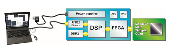
Digital signal processor (DSP) driven, equipped with 128 MB of DDR2 memory, USB2.0 interface and 1 Gbps Ethernet adapter. It is designed to be able to supports all chips and communication modes (serial and parallel) at the highest frequencies supported by the chip itself.
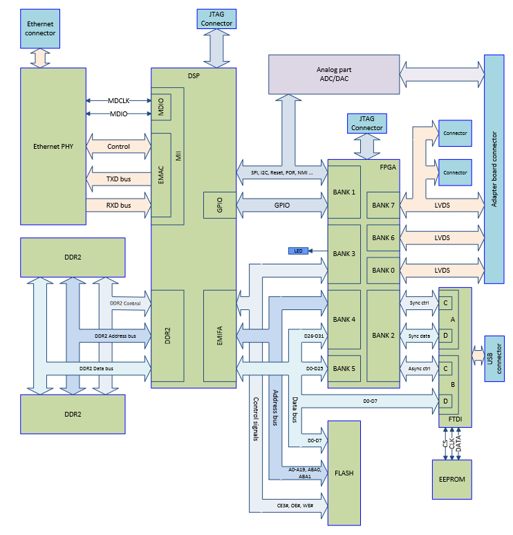
Basic block scheme of the RUIN.
All signals between Medipix and DSP go through the FPGA. It gives the possibility to implement new functionality easily by reprogramming the FPGA without need to change the hardware. Serial data from the Medipix detector are firstly de-serialized in the FPGA to decrease the processor load.
The RUIN is also equipped with eight 16-bit DACs , eight 16-bit ADCs , two JTAG connectors for programming DSP and FPGA, and two general purpose connectors (20 pins and 40 pins) containing SPI , I2C , ADC inputs and DAC outputs.
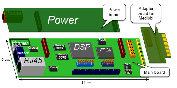
To be more flexible it was decided to use a modular system. The interface thus consists of three parts:
• Main board with logic (processor, FPGA, memory, USB etc.) and most of the connectors
• Power board with all power sources and power management
• Changeable Adapter board for Medipix which allows using more than one type of Medipix chipboards
Modular system of the RUIN. It consists of three parts: Main board, Power board and Adapter board for Medipix.
Development
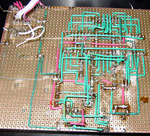
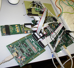
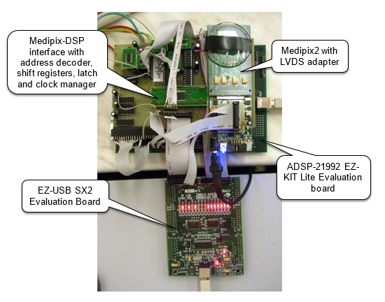
At first, the concept was built with the use of Analog devices ADSP-21992 EZ-KIT Lite evaluation board as DSP, Cypress SX2 evaluation board as USB2.0 interface, and CMOS logic interface between Medipix and DSP for the first prototyping, testing and debugging. Hardware design, programming, testing and proofing of this concept was the subject of my diploma thesis.
First interface prototype testing setup
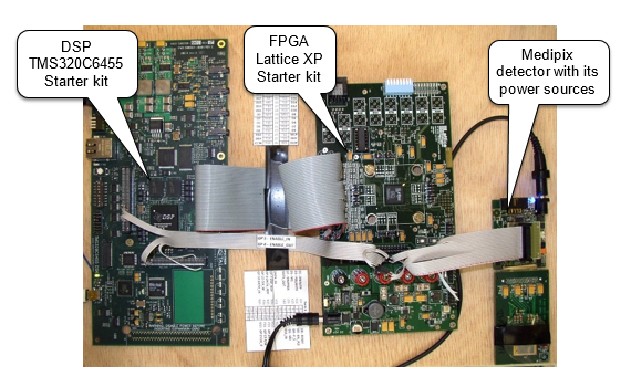
As the next step, the developed interface concept was designed with the new more powerful DSP TMS320C6455 by Texas instruments and FPGA Lattice XP instead of CMOS logic interface connecting Medipix with DSP. The first prototype with these new parts was realized with dedicated starter kits.
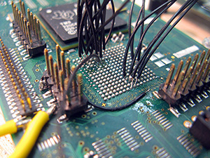
Verification of the designed interface concept realized with starter kits.Hardware debugging - BGA
After successful verification of the functionality of all parts important for the correct operation of the interface such as: communication between DSP and FPGA, USB communication, DDR2 memory reading and writing, flash memory reading and writing, communication with detector, the schema for ordering the PCB fabrication was designed. At first, two boards were assembled and communication with both of them via JTAG was tested. The first one with FPGA with necessary components only and the second one with DSP using XDS510 USB emulator by Spectrum Digital for communication with PC. Code Composer Studio IDE by Texas Instruments was used for programming and debugging the DSP. As a next step DSP and FPGA were assembled on the same board and tested together. Test of this interface prototype has been performed both with tester board allowing just signals evaluation and the Medipix detector itself. External power supplies were used.
After test some changes and improvements were proposed (usage of FT2232H by FTDI for USB communication instead of Cypress, type of some connectors, layout of the parts and connectors) and new version of prototype as well as the power sources board were designed, fabricated, assembled and tested.
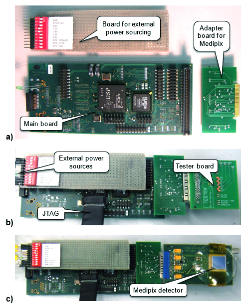
RUIN – first prototype of the PCB version: a) Consists of three parts: Main board, Board for external power sourcing and Adapter board for Medipix, b) with tester board c) with Medipix detector.
Results
The RUIN prototype based on TMS320C6455 DSP and FPGA Lattice XP was built and successfully tested. Testing firmware for DSP (in C++ programming language) and for FPGA (in VHDL) was developed and all the functionality crucial for the correct operation of the interface was approved:
• Flashing firmware to the assembled flash memory and correct loading to the DSP after power on.
• Communication with Medipix detector (read write FSR, read write matrix, open/close shutter)
• Saving and loading data to/from DDR2 memory.
• Communication with PC via USB interface.
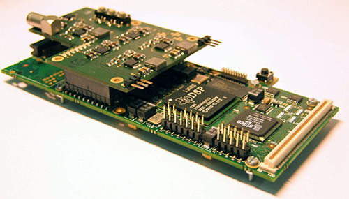
RUIN prototype (main board and power board).